



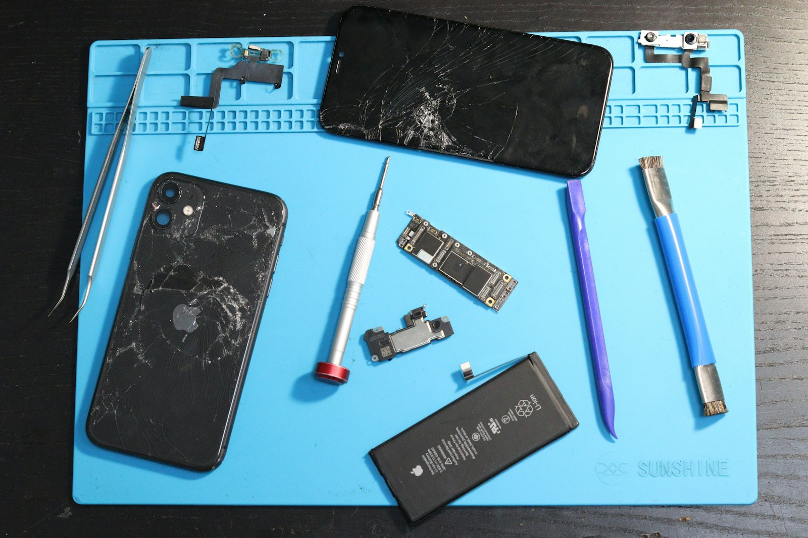





Pick up the phone in your pocket and try to trace where its main processor came from. It was probably designed in California, laid out with specialized design software, printed on a silicon wafer in Taiwan using a machine built in the Netherlands, cut and packaged somewhere in Asia, then assembled into a phone in yet another country. That’s the semiconductor supply chain in miniature: the chip crossed several borders before you ever turned it on.
That arrangement worked well for decades. It was cheap, efficient and almost invisible. Then a pandemic, an AI boom and a geopolitical standoff over Taiwan turned the semiconductor supply chain into one of the most watched industries on earth. Global chip sales hit roughly US$792 billion in 2025, up about 26%, and the Semiconductor Industry Association expects close to US$1 trillion in 2026.
Here’s how the pieces fit together, who controls the choke points, and where Canada, which most people never associate with chips, actually fits in.
Three jobs, three very different businesses
The single most useful idea for understanding the semiconductor supply chain is that “making a chip” is really three separate jobs, often done by different companies on different continents.
Design
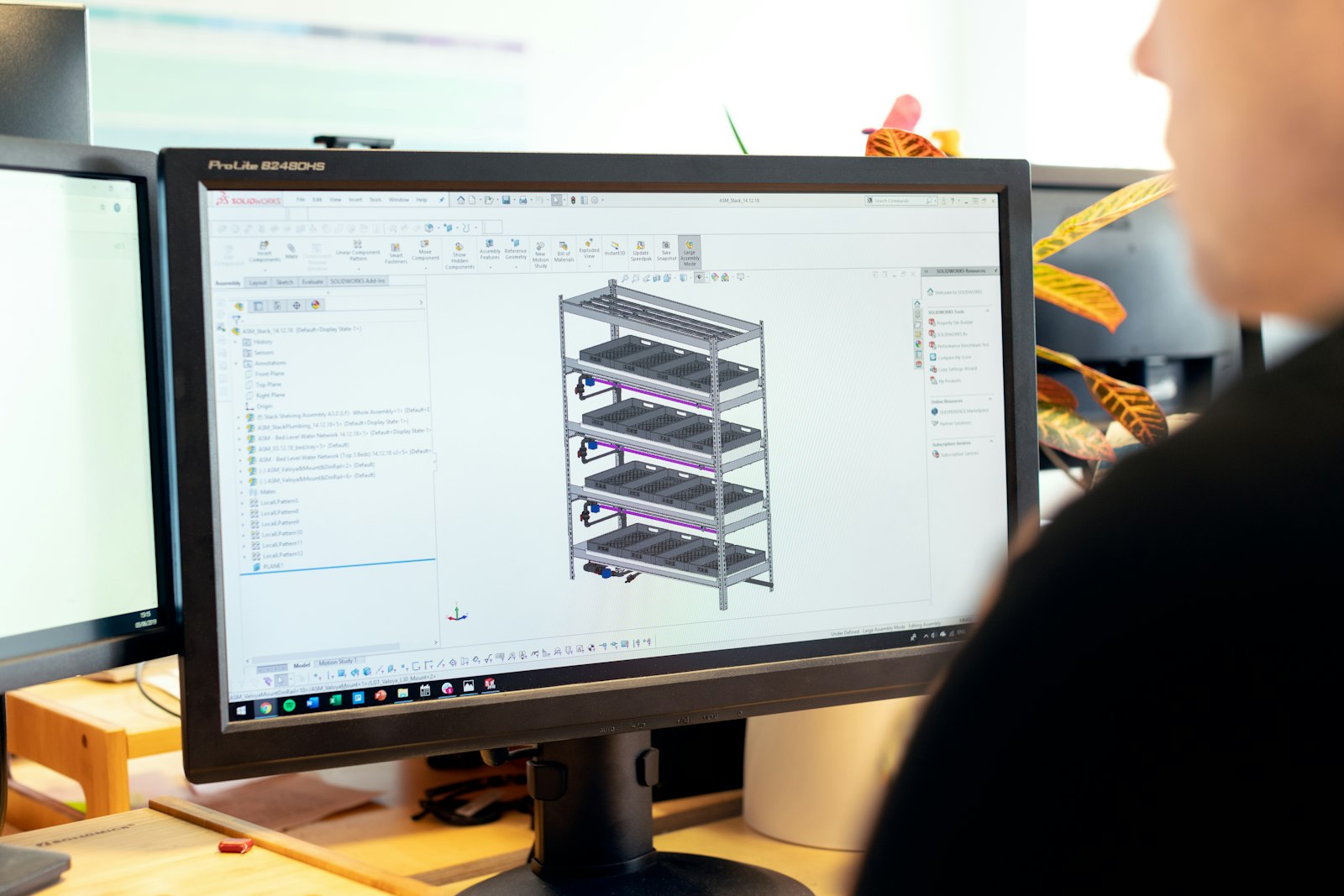
Companies such as Nvidia, Apple, AMD and Qualcomm decide what a chip does and lay out its billions of transistors. Most of them are “fabless”: they own no factories. They rely on electronic design automation (EDA) software and often license ready-made building blocks, such as processor cores, from other firms. Design is where the margins are highest and the capital costs lowest, which is why it is also the part of the industry where startups can still compete.
Fabrication
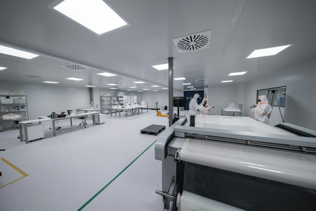
Fabrication, or “front-end” manufacturing, is where a design is etched onto silicon wafers in a fab, a building that can cost US$20 billion or more and is cleaner than an operating room. Pure-play foundries like TSMC manufacture other companies’ designs. Integrated device manufacturers (IDMs) such as Intel and Samsung design and make their own chips, and increasingly sell manufacturing to outsiders too.
Packaging and testing
A finished wafer is not a usable product. “Back-end” work cuts it into individual dies, tests them, and seals them in packages that connect to circuit boards. Much of this is handled by outsourced assembly and test (OSAT) firms such as ASE and Amkor, with Taiwan the biggest player. For years this was treated as the low-value, commoditized end of the business. That has changed fast, and it is where the AI story gets interesting.
The foundry race: TSMC, Samsung and a rebooted Intel
TSMC holds roughly 70% of the global foundry market and makes nearly all of the world’s most advanced logic chips. Its 2025 revenue came to about US$122 billion. The company moved to its 2-nanometre process, which uses a new “gate-all-around” transistor design, in late 2025. If you use an iPhone, a high-end Android phone or an Nvidia AI accelerator, the core silicon almost certainly came out of a TSMC fab.
Samsung is the only other company producing at the leading edge at meaningful scale, and it began 2nm production in 2025. It still trails TSMC by a wide margin in outside customers, and its fab project in Taylor, Texas, first announced in 2021 as a US$17 billion investment, is a test of whether it can close the gap.
Intel is the comeback story, or at least the attempted one. Under CEO Lip-Bu Tan, appointed in March 2025, the company cut roughly 24,000 jobs and shelved planned European fabs. It launched its Panther Lake laptop chips at CES in January 2026, built largely on its own 18A process, the first serious sign that its manufacturing roadmap is back on track. Nvidia invested US$5 billion in Intel in September 2025 to co-develop data centre and PC processors. And, unusually, Washington became a major shareholder (more on that below).
ASML and the most important machine you’ve never seen
Every leading-edge chip passes through a single choke point: extreme ultraviolet (EUV) lithography. These machines bounce light with a wavelength of 13.5 nanometres off ultra-precise mirrors to print the finest features on a chip. Only one company sells them: ASML, based in Veldhoven in the Netherlands.
ASML’s standard EUV tools cost up to about US$200 million each, and its newer High-NA systems around US$370 million. The machines rely on optics from Germany’s Carl Zeiss and a light source developed by Cymer, the San Diego company ASML bought in 2012. In other words, even the “Dutch” monopoly is a multinational supply chain of its own. ASML’s 2024 revenue was about €28.3 billion, and according to public company data it holds roughly 83% of the overall lithography market.
That monopoly makes ASML a geopolitical lever. Nobody can build a leading-edge fab without its machines, which is exactly why export controls focus on it.
Packaging: the new bottleneck for AI
The AI boom has turned packaging from an afterthought into a constraint. Modern AI accelerators are not single chips. They are several “chiplets” plus stacks of high-bandwidth memory, wired together on an interposer so data can flow between them at enormous speed. TSMC’s version of this technique, called CoWoS (chip-on-wafer-on-substrate), has been in such short supply that it has limited how many Nvidia GPUs reach the market. TSMC has been expanding CoWoS capacity by about 60% a year through 2026.
This matters because it shifts the geography of value. A country that can only do traditional back-end assembly sits at the cheap end of the chain. A country that can do advanced packaging becomes part of the AI hardware story. That’s the opening Canada is trying to use.
Export controls: the chip war in practice
Since October 2022, the United States has restricted China’s access to advanced AI chips, chipmaking tools and the engineers who support them. In early 2023 the controls went multilateral, with Japan and the Netherlands agreeing to restrict their own equipment. The Dutch government added licence requirements for advanced ASML tools in September 2023 and tightened them again in January 2025. EUV machines have never been shipped to China.
The rules keep shifting. Nvidia has designed a string of China-specific chips to fit under each new threshold, and Washington has alternated between blocking and permitting them. In May 2026, the US Commerce Department cleared ten Chinese companies, including Alibaba, Tencent, ByteDance and JD.com, to buy Nvidia’s H200 accelerators. Beijing, meanwhile, had reportedly told its own firms to avoid the chips unless strictly necessary, preferring to build demand for domestic alternatives such as Huawei’s Ascend line.
China’s progress is real but uneven. SMIC has produced 7nm-class chips for Huawei phones without EUV, and Reuters reported in December 2025 that China had quietly completed a prototype EUV machine in Shenzhen, with working chips not expected before 2028 to 2030. Smuggling is a persistent leak; in May 2026, Taiwanese authorities detained three people over alleged Nvidia chip shipments to China routed via Japan.
The CHIPS Act and the reshoring push
The US response on the supply side is the CHIPS and Science Act of 2022, which set aside US$52.7 billion for semiconductors, including US$39 billion in manufacturing incentives and a 25% investment tax credit. Big awards went to Intel, TSMC (US$6.6 billion), Samsung (US$6.4 billion) and Micron (US$6.1 billion).
The Trump administration kept the law but changed how it is used. In August 2025, the government converted grants into a 9.9% equity stake in Intel at US$20.47 a share, paid for with about US$11.1 billion in CHIPS money, as records of the act’s implementation show. It also raised the manufacturing tax credit by ten percentage points and, in May 2026, extended the equity-for-grants model to quantum computing firms.
Has it worked? Partly. TSMC has raised its planned Arizona investment to US$165 billion. Its first Phoenix fab has been producing 4nm chips since early 2025, a second fab is slated for 3nm volume production in the second half of 2027, and Apple says it will buy more than 100 million chips made at TSMC Arizona in 2026. Two advanced packaging plants are planned for the site, with Amkor as a partner. But the most advanced nodes still debut in Taiwan, and US fabs remain more expensive to run.
Where Canada fits in the semiconductor supply chain
Canada doesn’t make leading-edge chips and isn’t likely to. What it has is a niche that suddenly matters: packaging and testing.
IBM’s plant in Bromont, Quebec, about an hour east of Montreal, is one of the largest chip assembly and test facilities in North America and has been doing semiconductor work for more than 50 years. Next door sits C2MI, Canada’s largest microelectronics R&D centre, founded with IBM, Teledyne DALSA and the Université de Sherbrooke. In November 2025, Ottawa announced up to $210 million through its Strategic Response Fund toward a $662 million project to expand packaging and commercialization capacity at the two sites, according to the federal announcement. The government says the work will create 75 jobs and maintain more than 1,000 in the region, with a focus on AI, high-performance computing, quantum and defence. C2MI also aims to become what it calls the world’s first open foundry for superconducting quantum chips, and Quebec pledged support for its expansion in July 2026.
Beyond Bromont, Canada’s realistic strengths are in design and talent rather than wafer fabrication. Like most chip designers worldwide, Canadian hardware startups rely on foreign foundries to turn their designs into silicon, which means the export rules and capacity crunches described above apply to them too.
The policy question for Canada is whether to chase fabs it can’t afford or double down on the parts of the chain where it already has an edge. Given what a single leading-edge fab costs, Bromont-style specialization looks like the more realistic bet.
What this means for you
You don’t need to run a chip company for the semiconductor supply chain to affect you. A few practical takeaways:
- Hardware founders: foundry capacity at the leading edge is booked by giants. Mature nodes (28nm and above) are easier to access and cheaper. Plan for long lead times, and look at Canadian prototyping resources such as C2MI before assuming you need to go abroad.
- Buyers of AI compute: GPU supply is shaped as much by packaging capacity and export politics as by demand. Expect pricing and availability to stay lumpy.
- Anyone exporting tech: US export rules can reach products with American content even when they’re sold from Canada. If you ship advanced chips or servers internationally, get trade-compliance advice early. (This is general information, not legal advice.)
- Consumers: when an industry concentrates this much risk in one island and one toolmaker, any disruption eventually ripples into the price and availability of your next phone or laptop.
The big lesson of the last five years is that the chip world is not one industry but a relay race with very few runners at each leg. Whoever controls a leg, whether it’s ASML’s lithography, TSMC’s fabs or the packaging lines that bolt AI chips together, holds real power. Canada’s best play is to own a leg, even a short one.
Sources and further reading
- Government of Canada: Canada invests in the semiconductor sector in partnership with IBM Canada and C2MI (Nov. 2025)
- C2MI: MiQro Innovation Collaborative Centre, Bromont
- CHIPS and Science Act: funding, awards and 2025 changes
- TSMC Arizona: investment and fab timeline
- ASML Holding: EUV lithography and export restrictions
- Semiconductor industry: business models and 2025 market data
- Semiconductor industry in China: export controls and domestic progress
- Intel Panther Lake and the 18A process